MI355X architecture and system topology
Chapter 1 of How to Scale Your Model on AMD (Chapter 0: Intro | Chapter 2: The JAX/ROCm Stack)
The gfx950 execution, memory, precision, and interconnect limits that govern JAX training on one MI355X or one eight-GPU node.
The AMD Instinct MI355 belongs to AMD’s CDNA family of accelerators for HPC and AI workloads, serving a role equivalent to NVIDIA’s H100 and H200. Its architecture is designed around the computational patterns common in modern AI models, with an emphasis on high-throughput matrix multiplication and matrix cores that perform these operations efficiently.
Inside an MI355X
MI355X is an OCP (Open Compute Project) Accelerator Module based on AMD CDNA 4.
Its LLVM target is gfx950. This section follows one accelerator through its
chiplet package and down to the wavefronts that execute instructions, then
relates that physical hierarchy to the logical device presented to JAX.
Package organization
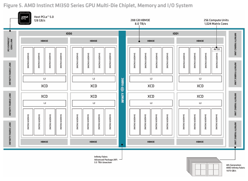
The package contains two I/O dies (IODs), eight Accelerator Complex Dies (XCDs), eight HBM3E stacks, and 256 active Compute Units (CUs). It has 288 GB of HBM3E and a 2.4 GHz peak engine clock. These identities come from the MI355X GPU product brief and the CDNA 4 architecture white paper.
Compute hierarchy
The execution hierarchy is:
| Scope | Contents |
|---|---|
| MI355X OAM | two IODs, eight XCDs, and eight HBM3E stacks |
| IOD | HBM controllers, Infinity Cache, PCIe, and external Infinity Fabric |
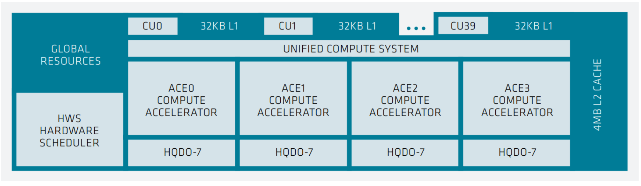
| XCD | 36 physical CUs, 32 active, sharing 4 MB of L2 |
| Active CU | four SIMD vector units, four Matrix Cores, scalar and memory pipelines, 32 KiB L1 vector cache, and 160 KiB LDS |
| Full OAM memory | 288 GB HBM3E |
Across the package, 8 XCDs × 32 active CUs/XCD = 256 CUs. There are four SIMDs
and four Matrix Cores per CU, giving 1,024 of each across the OAM. Note that an XCD and a
Shader Engine are not the same unit. The XCD is a compute chiplet containing CUs,
cache, and scheduling resources.
A CU has 64 stream processors arranged as four SIMD16 vector pipelines. A Wave64 contains 64 logical work-items and is issued through a SIMD16 pipeline as four 16-lane quarter-waves. MFMA is still a wave-level operation: all 64 logical lanes contribute register fragments to one matrix instruction. A HIP workgroup or an XLA-generated GPU block can contain several waves. For example, a 256-thread workgroup contains four waves. The hardware can hold at most eight resident waves per SIMD, or 32 per CU, if registers, LDS, and other resources permit.
For readers coming from CUDA, the small translation table is:
| NVIDIA term | AMD CDNA 4 term | MI355X |
|---|---|---|
| Streaming Multiprocessor | Compute Unit | 256 per OAM |
| warp | wavefront | 64 threads, not 32 |
| CUDA core | SIMD execution lane | 16 physical lanes per SIMD; 64 stream processors per CU |
| Tensor Core | Matrix Core using MFMA | four per CU |
| thread block | workgroup | one or more waves |
| shared memory | LDS | 160 KiB per CU |
| local memory spill | scratch | backed outside the register file |
| NVLink | xGMI over Infinity Fabric | seven direct peer links |
The ROCm device stack
The physical hierarchy above reaches JAX through the Linux driver, ROCm userspace runtimes, and XLA’s ROCm backend. The diagram shows the device path; Chapter 2 follows the separate compilation path that produces the executable.
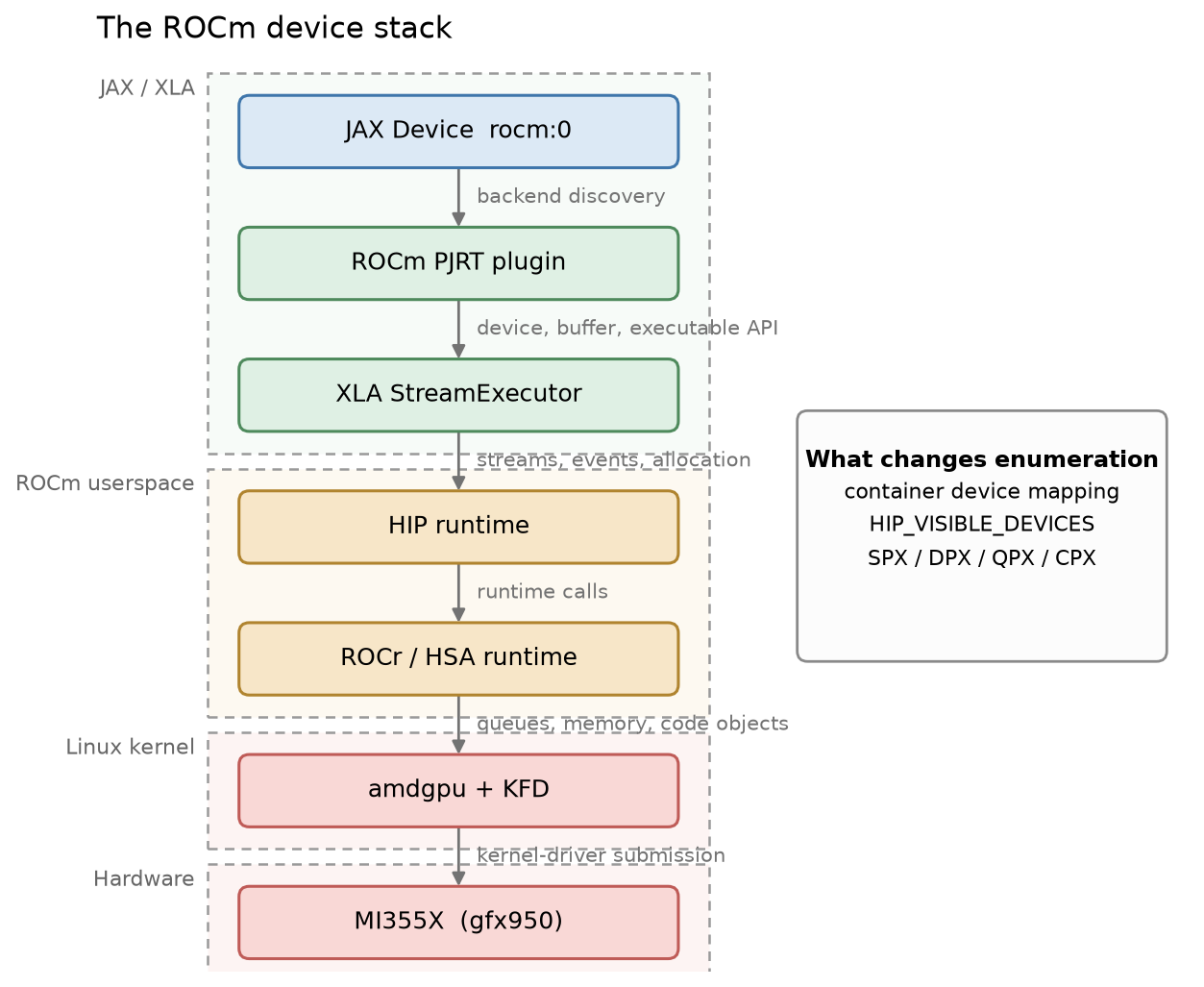
Each OAM has one PCIe Gen 5 x16 host or I/O connection; peer traffic within the UBB uses Infinity Fabric instead. JAX therefore presents one device abstraction over paths with very different bandwidth and locality.
Matrix execution
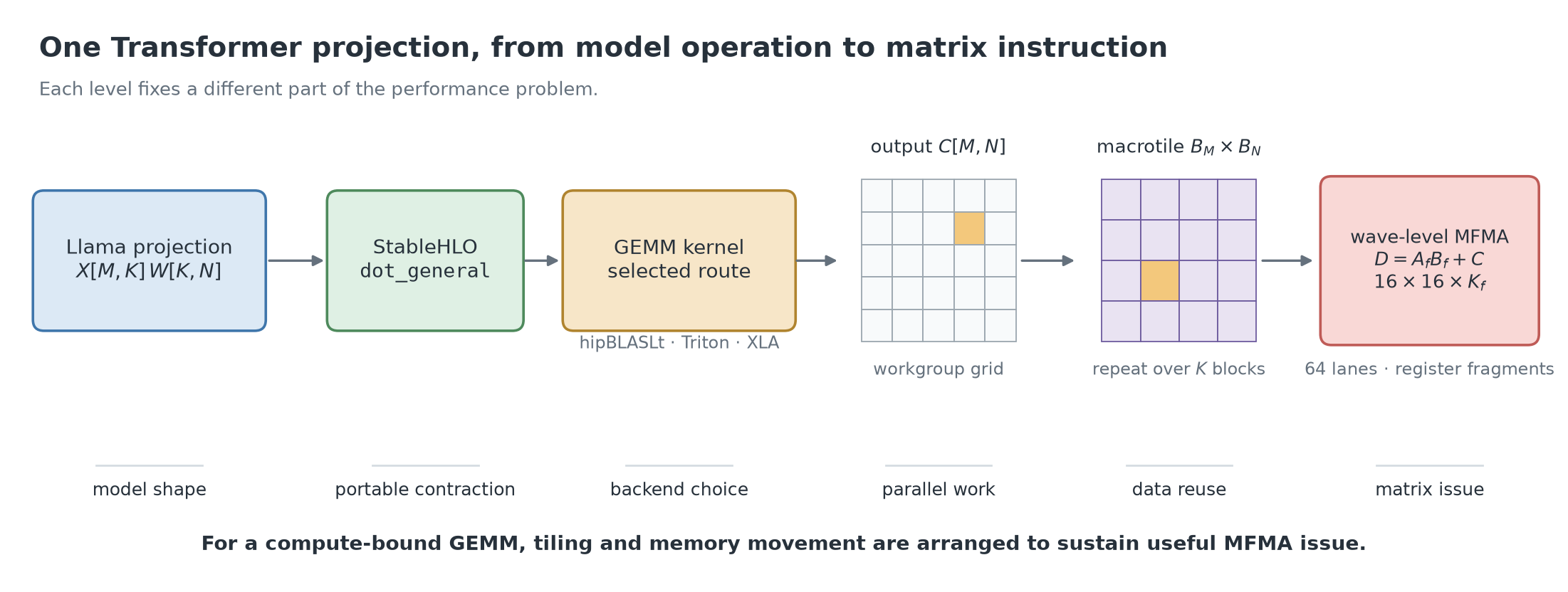
Transformer training spends most of its FLOPs in matrix multiplications. For a compute-bound matrix kernel, MFMA is the innermost compute primitive. Kernel optimization chooses parallel work, tiles, data movement, and schedules that keep useful MFMA instructions issuing.
Example: Lowering a projection matrix to a GEMM, to MFMA instructions
A Transformer linear projection can be written as
\[Y[M,N]=X[M,K]W[K,N].\]For an MLP up-projection, $M$ is the number of local token rows, $K=D$ is the model width, and $N=F$ is the feed-forward width. These are the dimensions seen by the kernel after batching and sharding; a large global projection can become a much smaller local GEMM on each GPU.
JAX represents the contraction as dot_general. Chapter 2 follows the compiler
path in detail. At the GPU boundary, XLA can select a hipBLASLt library call, a
Triton implementation, or generated code. With a library call, the library
kernel owns the tiling and MFMA decomposition. With a generated route, the
compiler emits more of that structure itself. The resulting GPU kernel still
has to divide the GEMM into workgroups, stage operands, and accumulate output
tiles.
Blocked GEMM
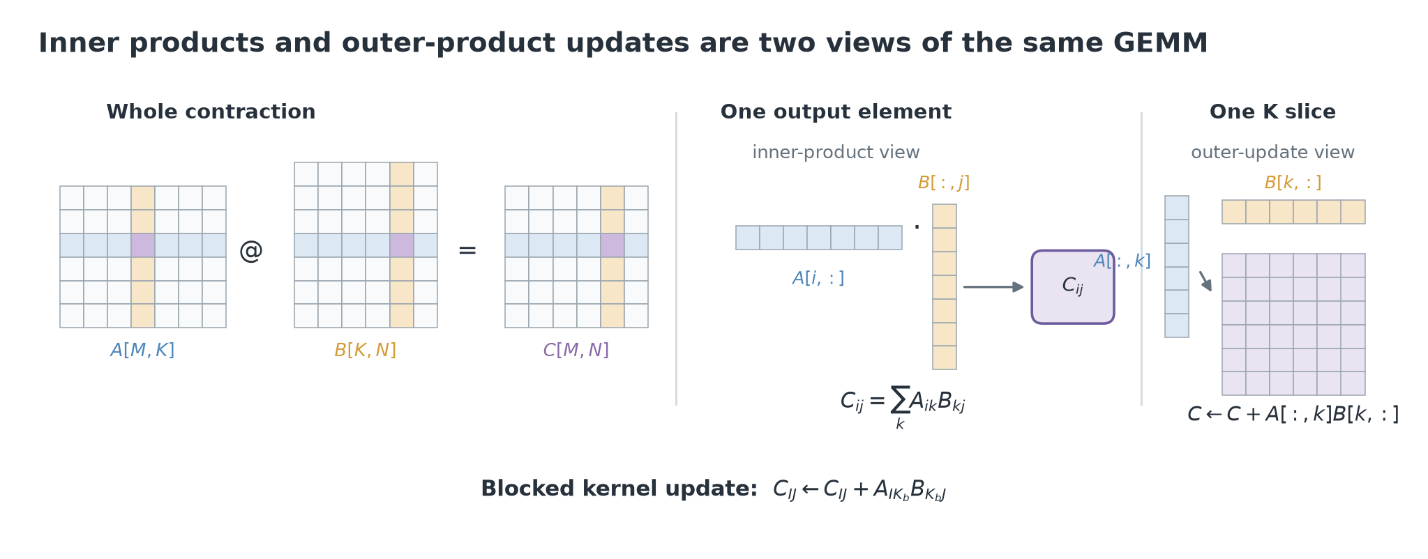
A kernel partitions the output matrix into macrotiles. A workgroup owns one output region $C_{IJ}$ and loops over blocks of the contracting dimension:
\[C_{IJ}\mathrel{+}=A_{IK_b}B_{K_bJ}.\]Each iteration loads an $A$ tile and a $B$ tile, stages them through LDS, and updates register-resident accumulators. Splitting $M$ and $N$ creates parallel workgroups; splitting $K$ creates repeated accumulation and operand reuse. The workgroup writes the output macrotile after all $K$ blocks have contributed.
Inner and outer views
Every scalar output is an inner product between one row of $A$ and one column of $B$:
\[C_{ij}=\sum_k A_{ik}B_{kj}.\]The same GEMM can be viewed one $K$ position at a time as an outer-product update:
\[C\mathrel{+}=A[:,k]B[k,:].\]These are two views of the same contraction. Tiling does not choose one over the other. Each output element accumulates a dot product, while each $K$ slice updates many output elements at once. A blocked GEMM groups several such positions into the matrix update $C_{IJ}\mathrel{+}=A_{IK_b}B_{K_bJ}$.
MFMA lane fragments
An MFMA applies the same matrix update at instruction scale:
\[D=A B+C,\qquad F_{\mathrm{tile}}=2mnk,\]where every multiply-accumulate counts as two floating-point operations. An MFMA is a wave-level operation: all 64 lanes provide register fragments of the input matrices and receive fragments of the output accumulator.
The instruction name states its logical shape. CDNA 4 adds BF16 and FP16 forms
with output tiles of $16\times16$ and $32\times32$, including 16x16x32 and
32x32x16 forms. Its low-precision scaled family includes
v_mfma_scale_f32_16x16x128_f8f6f4 and
v_mfma_scale_f32_32x32x64_f8f6f4. The exact operand layout is defined by the
CDNA 4 ISA.
The f32 in those names describes the accumulator. Low-precision inputs can
therefore contribute to FP32 partial sums before the kernel converts its stored
output to the requested dtype. The later precision experiments identify all
three roles: input format, accumulator format, and output format.
AMD’s
CDNA 4 FP8 GEMM guide
shows the lane mapping for a 16x16x128 FP8 instruction. Each of the 64 lanes
holds 32 FP8 elements from $A$, 32 from $B$, and four FP32 accumulator values.
Together the lanes update a $16\times16$ output tile:
An instruction tile is smaller than the region assigned to a workgroup. Several waves cooperate through LDS to build a macrotile. One published MI355X example assigns eight waves to a $256\times256\times128$ workgroup tile. Each wave issues many MFMA updates as the workgroup advances through its output and $K$ tiles.
Operands move from HBM or cache into an LDS staging tile, then into VGPR fragments consumed by MFMA. Partial sums remain in FP32 accumulator registers until the kernel writes the output.
For a compute-bound GEMM, the innermost throughput question is whether useful MFMA instructions can issue continuously:
- Are there enough output tiles to distribute work across 256 CUs?
- Do the local $M$, $N$, and $K$ dimensions fill efficient instruction tiles?
- Can LDS and VGPR movement keep the Matrix Cores supplied?
- Do tails, register pressure, spills, or bank conflicts reduce useful issue?
Shape tails
Matrix dimensions rarely arrive as one hardware instruction. A kernel tiles $M$, $N$, and $K$, then masks, pads, or sends incomplete edge tiles to a cleanup path. For tile sizes $T_M,T_N,T_K$, a simple padded-work estimate is
\[F_{\mathrm{padded}} = 2\left\lceil\frac{M}{T_M}\right\rceil T_M \left\lceil\frac{N}{T_N}\right\rceil T_N \left\lceil\frac{K}{T_K}\right\rceil T_K.\]If only $M$ has a tail, $M=257$, and the macrotile step is 32 rows, padding to 288 rows adds
\[\frac{288}{257}-1=12.1\%\]to this upper estimate. A predicated kernel may avoid some arithmetic while still paying for inactive lanes and less efficient memory transactions. This is why batch, sequence, hidden, and expert dimensions that look almost identical at the model level can select different kernels or show different utilization. No one tile divisibility rule covers every backend, rather you should inspect the selected kernel and profile the actual shape.
A useful TPU contrast
A TPU MXU is a comparatively large systolic array. Values flow through its
two-dimensional multiply-accumulate grid. MI355X distributes matrix execution
across 1,024 Matrix Cores in 256 CUs, and each MFMA starts with wave-lane
fragments. The JAX source can contain the same dot_general, but the utilization
problem differs:
- On a TPU, array dimensions and MXU tiling determine how well the systolic array is filled.
- On MI355X, MFMA shape, wave and workgroup tiles, register allocation, LDS staging, and the number of CUs receiving work all influence utilization.
The JAX Scaling Book TPU chapter explains the systolic side. This companion uses the same roofline method but substitutes the MI355X execution and memory limits.
The rest of a training kernel
Matrix Cores do not execute the whole step. CDNA 4 CUs also contain vector, scalar, memory, and control pipelines:
- SIMD vector instructions handle elementwise activations, optimizer updates, dtype conversion, normalization arithmetic, masking, and address-dependent work.
- Scalar instructions handle values uniform across a wave, including loop bounds, base addresses, and control decisions.
- Reductions combine lane values through shuffle or LDS stages. Larger reductions may require several workgroups or a device collective.
- Memory instructions move values among HBM, caches, LDS, and registers.
These paths explain why a $2\times$ matrix peak FLOPs does not imply a $2\times$ training-step speedup. This is Amdahl’s law: if a fraction $p$ of step time improves by a factor $s$, the largest end-to-end speedup with the remainder unchanged is
\[S_{\mathrm{step}}=\frac{1}{(1-p)+p/s}.\]If GEMMs account for 85% of a hypothetical step and they experience a $2\times$ speedup, then the theoretical training step speedup becomes:
\[S_{\mathrm{step}}=\frac{1}{0.15+0.85/2}=1.74,\]A profile determines the workload-specific value of $p$ by measuring time spent in attention softmax, normalization, optimizer work, routing, launch gaps, collectives, and other work outside the accelerated GEMMs.
Memory hierarchy
| Level | MI355X capacity | Scope | Training role |
|---|---|---|---|
| VGPR and AccVGPR | 512 32-bit entries per lane | one SIMD; allocated per wave | operands, accumulators, live values |
| LDS | 160 KiB | one CU; shared by a workgroup | software-managed staging and cross-wave exchange |
| L1 vector cache | 32 KiB | one CU | cached vector and global loads |
| L2 | 4 MiB | one XCD, 32 active CUs | coalesces traffic before Infinity Fabric |
| Infinity Cache | 256 MiB | one OAM, shared across eight XCDs | memory-side last-level cache |
| HBM3E | 288 GB at 8 TB/s peak | one OAM | parameters, optimizer state, activations, and workspaces |
ROCm’s GPU specification table also lists the 32 KiB vector L1, 4 MiB of L2 per XCD, 256 MiB last-level cache, and 512 KiB total VGPR storage per CU. The table above expresses the register budget in the per-lane unit needed for occupancy calculations.
Cache scope and chiplet locality
The cache labels alone are not enough. A value reused by waves on one CU can remain in its L1. Work spread across CUs on one XCD can share that XCD’s L2. Traffic crossing an XCD boundary leaves that L2 and enters the on-package Infinity Fabric toward the IODs, Infinity Cache, or HBM controllers.
In SPX mode, workgroups are distributed across XCDs; ordinary JAX code does not pin an HLO operation to a chosen XCD. Library kernels may use XCD-aware tile ordering, but as the programmer, you should not assume that two successive workgroups share an L2 slice. Cache reuse is a kernel and schedule property that must be checked with counters.
The 256 MiB Infinity Cache is shared at package scope, but it does not turn HBM into an on-chip scratchpad. A 70-billion-parameter model occupies about 140 GB in BF16, roughly 530 times the cache capacity. Training kernels still depend on tiling, prefetch, and high HBM bandwidth.
Direct global to LDS loads
CDNA 4 can move data from the global-memory path directly into LDS
without first staging the payload in VGPRs. AMD documents this through the
llvm.amdgcn.raw.buffer.load.lds intrinsic and the wider CDNA 4
GLOBAL_LOAD_LDS path. The destination is still LDS; waves later read the
fragments into registers before MFMA.
Direct-to-LDS can reduce temporary VGPR use and remove explicit LDS stores. It does not remove synchronization, guarantee a conflict-free LDS layout, or make the data immediately available to MFMA. A tuned pipeline overlaps the load of a future K tile with MFMA on the current tile, then waits at the point where the new tile is consumed.
Resource pressure and occupancy
A kernel can be ready to execute but unable to place another wave on a SIMD because one resource is exhausted. The main limits are:
- regular VGPR and accumulator-register use per wave;
- scalar-register use per wave;
- LDS bytes per workgroup;
- workgroup and barrier slots.
On gfx950, regular VGPRs and AccVGPRs share one 512-entry-per-lane budget. Each type can use at most 256 entries per wave, with a flexible split, but they are not two independent 512-entry pools. The register limit in waves per SIMD is approximately
\[W_{\mathrm{VGPR}} = \left\lfloor \frac{512}{R_{\mathrm{VGPR}}+R_{\mathrm{AccVGPR}}} \right\rfloor,\]after allocation-granularity rounding. LDS is allocated per workgroup, so its first result is workgroups per CU:
\[G_{\mathrm{LDS}} = \left\lfloor \frac{160\ \mathrm{KiB}}{L_{\mathrm{workgroup}}} \right\rfloor.\]Convert all limits to waves per SIMD, take the minimum, and constrain to eight. The MI355X occupancy guide derives the conversion for different workgroup sizes.
More occupancy can hide latency because the scheduler can issue another ready wave. More instruction-level parallelism (ILP) can hide the same latency inside one wave by keeping independent loads or accumulators in flight. Larger tiles usually increase ILP and data reuse but consume more registers. The target is enough parallel work to feed the limiting pipeline, not the highest possible occupancy percentage.
Worked occupancy example
Consider the example from AMD’s occupancy guide: a 256-thread, four-wave MXFP8 workgroup uses 128 total VGPR entries per lane, 50 SGPRs per wave, and 32 KiB of LDS.
The register ceiling is
\[W_{\mathrm{VGPR}}=\left\lfloor\frac{512}{128}\right\rfloor=4 \quad\text{waves per SIMD}.\]The LDS holds
\[G_{\mathrm{LDS}}=\left\lfloor\frac{160}{32}\right\rfloor=5 \quad\text{workgroups per CU}.\]Each four-wave workgroup places one wave on each of the four SIMDs, so the LDS limit converts to five waves per SIMD. SGPRs and workgroup slots do not bind in the published example. The register limit wins:
\[\mathrm{occupancy}=\frac{\min(4,5,8)}{8}=50\%.\]That 50% is a resource ceiling, not a prediction of throughput. A matrix kernel with enough ILP may keep the Matrix Cores busy at lower occupancy; a memory-latency-bound kernel may need more resident waves.
Spills and bank conflicts
If live values exceed the register allocation, the compiler can spill them to scratch memory. Scratch has a private-address-space programming model, but it is not a hidden extension of the register file. Spill loads and stores enter the memory hierarchy and can add dependencies in a hot loop. Kernel names, compiler resource reports, ISA metadata, and profiler counters are the evidence for a spill diagnosis.
LDS pressure has two forms. Capacity pressure reduces resident workgroups. Access pressure occurs when several lanes address the same bank in one phase. CDNA 4 LDS has 64 banks and up to 256 bytes per clock of read bandwidth. A poor lane layout serializes bank-conflicting accesses even when capacity and occupancy look healthy. Padding or swizzling the LDS tile can change the bank mapping, but the benefit is shape- and schedule-dependent.
CDNA4 Native precision formats
The hardware supports more formats than a training recipe should use. A format is useful only when the JAX-to-kernel path selects the corresponding instruction and the training run passes its numerical checks. Hardware support is necessary, not sufficient.
BF16 is the baseline format for this book. It keeps FP32’s eight-bit exponent with fewer significand bits, which makes it easier to use for training than FP16’s narrower exponent range. BF16 and FP16 have the same published MI355X matrix peak. Both commonly accumulate into FP32.
FP32 remains important for accumulation and sensitive state even though its matrix peak is much lower. Optimizer moments, reductions, logits, and selected normalization operations may stay in FP32 while the large GEMMs use a compact input format.
OCP FP8
gfx950 uses the OCP FP8 encodings:
- E4M3 has one sign bit, four exponent bits, and three mantissa bits.
- E5M2 has one sign bit, five exponent bits, and two mantissa bits.
E4M3 trades exponent range for precision; E5M2 trades precision for exponent
range. They are not bit-compatible with the FNUZ FP8 variants used by gfx942.
Checkpoint and scale metadata must therefore identify the encoding, not merely
say fp8. The
OCP FP8 specification
defines the encodings.
FP8 training also needs a scaling policy. The scale may be chosen per tensor or per channel and updated from current or delayed amax statistics. Those are software and numerical decisions covered in the precision chapter; the hardware fact here is that MI355X can execute OCP FP8 matrix instructions at twice its BF16 matrix rate.
Microscaling formats
CDNA 4 adds native MXFP8, MXFP6, and MXFP4 matrix instructions. The OCP Microscaling Formats specification groups 32 values under one E8M0 scale. E8M0 stores a power-of-two scale as an eight-bit biased exponent. The element encodings are:
| Format | Element encoding | Scale block | Effective storage including one scale |
|---|---|---|---|
| MXFP8 | E4M3 or E5M2 | 32 values | $8+8/32=8.25$ bits/value |
| MXFP6 | E3M2 or E2M3 | 32 values | $6+8/32=6.25$ bits/value |
| MXFP4 | E2M1 | 32 values | $4+8/32=4.25$ bits/value |
The effective-storage column excludes tensor padding, alignment, and auxiliary metadata. A block whose length is not a multiple of 32 needs padding or a tail representation. The shared scale preserves more local range than one scale for a whole tensor, but it does not restore the precision discarded by a four- or six-bit element.
Scaled MFMA instructions consume element blocks and their scale information as part of the matrix operation. Whether JAX reaches those instructions through Transformer Engine, AITER, Triton, or another custom call is a software-stack question. Chapter 2 shows how to prove the route rather than infer it from a configuration name.
Dense and sparse peaks
The table uses the 2.4 GHz MI355X figures. A sparse peak requires the hardware-supported structured pattern and a kernel that uses the sparse path. Ordinary dense transformer weights use the dense column.
| Matrix input format | FLOPs per clock per CU | Dense peak per OAM | Published structured-sparse peak |
|---|---|---|---|
| FP32 | 256 | 157.3 TFLOP/s | not listed |
| FP16 | 4,096 | 2.5166 PFLOP/s | 5.0332 PFLOP/s |
| BF16 | 4,096 | 2.5166 PFLOP/s | 5.0332 PFLOP/s |
| OCP FP8 | 8,192 | 5.0332 PFLOP/s | 10.0663 PFLOP/s |
| MXFP8 | 8,192 | 5.0332 PFLOP/s | not listed in the product table |
| MXFP6 | 16,384 | 10.0663 PFLOP/s | not listed in the product table |
| MXFP4 | 16,384 | 10.0663 PFLOP/s | not listed in the product table |
The dense BF16 ceiling can be rebuilt from architectural factors:
\[\begin{aligned} C_{\mathrm{BF16}} &=256\ \mathrm{CUs} \times4096\ \frac{\mathrm{FLOPs}}{\mathrm{clock\cdot CU}} \times2.4\times10^9\ \frac{\mathrm{clocks}}{\mathrm{s}}\\ &=2.5165824\times10^{15}\ \mathrm{FLOP/s}\\ &\approx\mathbf{2.5166\ PFLOP/s}. \end{aligned}\]The same reconstruction gives 5.0332 PFLOP/s for FP8 and MXFP8, and 10.0663 PFLOP/s for MXFP6 and MXFP4. Do not use a sparse number in MFU unless the workload and kernel actually use structured sparsity.
Partition modes
MI355X can split its eight XCDs into logical accelerator partitions. Compute partitioning and HBM NUMA partitioning are separate controls. AMD’s published MI355X workload table lists:
| Compute mode | Logical GPUs per OAM | XCDs per logical GPU | HBM per logical GPU | Published NPS pairing |
|---|---|---|---|---|
| SPX | 1 | 8 | 288 GB | NPS1 |
| DPX | 2 | 4 | 144 GB | NPS2 |
| QPX | 4 | 2 | 72 GB | NPS2 |
| CPX | 8 | 1 | 36 GB | NPS2 |
The
ROCm workload guide
provides these MI355X profiles. Exact support is firmware-dependent, so
amd-smi partition --accelerator on the target host is authoritative. The
AMD SMI partitioning guide
explains the logical-device model.
JAX sees the logical GPUs exposed by the driver. Thus one CPX-partitioned OAM
can enumerate as eight devices, while the same OAM in SPX enumerates as one.
The peak compute, memory capacity, and cache scope available to one JAX device
have changed even though jax.device_count() increased.
This book assumes SPX with NPS1 for full-OAM training. DPX with NPS2 is AMD’s efficiency recommendation for partitioned MI355X workloads, but it is not a general recommendation to split a large JAX training job. Always record partition mode with a benchmark. A clean $2\times$, $4\times$, or $8\times$ error in a roofline often means the calculation assumed SPX while the process saw a partition.
Capacity bandwidth and the BF16 roofline
One MI355X has 288 GB of HBM3E and 8 TB/s peak HBM bandwidth. Capacity answers whether the local shard, activations, compiler temporaries, and workspaces fit. Bandwidth limits kernels that do too little arithmetic per byte fetched from HBM.
For peak compute $C$, bandwidth $\beta_{\mathrm{HBM}}$, and arithmetic intensity $I=F/Q$, the ideal roofline is
\[P\leq\min\left(C,\ I\beta_{\mathrm{HBM}}\right),\]or, as a time lower bound,
\[t\geq\max\left(\frac{F}{C},\frac{Q}{\beta_{\mathrm{HBM}}}\right).\]The dense BF16 machine balance is
\[I^*_{\mathrm{BF16}} =\frac{2.5165824\times10^{15}}{8.0\times10^{12}} =314.5728\ \mathrm{FLOP/byte} \approx\mathbf{315\ FLOP/byte}.\]A BF16 matrix operation below roughly 315 FLOP/byte cannot reach the dense BF16 compute ceiling even with a perfect memory implementation. The ridge is not a cliff, and real kernels lose bandwidth and compute efficiency on both sides.
Chapter 3 applies this ratio to concrete training projections and derives the corresponding token-row threshold. This chapter only supplies the hardware side of that calculation.
Eight-GPU scale-up domain
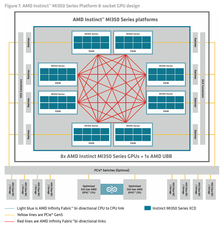
The MI355X UBB 2.0 places eight OAMs in a one-hop, fully connected mesh. Every GPU has one dedicated xGMI link to each of its seven peers. There is no scale-up switch between them. A ninth GPU would need to be reached through a scale-out network.
The topology is valuable for tensor, expert, and fully sharded parallelism because every pair can communicate directly. It also sets a hard placement boundary: a parallelism axis of size eight can remain inside xGMI; a larger axis crosses NICs.
Directional bandwidth
Each xGMI link is 16 lanes at 38.4 Gb/s per lane:
\[\beta_{\mathrm{xGMI,one\ direction}} =\frac{16\times38.4\ \mathrm{Gb/s}}{8} =\mathbf{76.8\ GB/s}.\]Because transmit and receive directions are independent, AMD also publishes 153.6 GB/s bidirectional per link. Summing seven links gives:
\[\beta_{\mathrm{egress}}=7(76.8)=537.6\ \mathrm{GB/s},\]and 1,075.2 GB/s only when transmit and receive are added together. A cost model for bytes sent in one direction must use 76.8 GB/s per peer link or 537.6 GB/s aggregate egress, not the doubled marketing total.
Sending 1 GB to one peer has an ideal serialization lower bound of
\[\frac{1\ \mathrm{GB}}{76.8\ \mathrm{GB/s}}=13.0\ \mathrm{ms}.\]This excludes protocol overhead, synchronization, software latency, and any collective algorithm. It is not a measured RCCL time.
Partial participation
The 537.6 GB/s aggregate assumes traffic can use all seven peer links at once. A two-GPU operation can use only the one physical link between those GPUs. A four-GPU subgroup has only three participating peer links per GPU. The unused links do not combine into a faster link to one destination.
If one GPU sends 1 GB concurrently to each of seven peers, the ideal time is still
\[\frac{7\ \mathrm{GB}}{7(76.8)\ \mathrm{GB/s}}=13.0\ \mathrm{ms},\]because the seven pairwise links operate in parallel. That equality describes the physical complete graph. RCCL may choose a ring, tree, or specialized algorithm with different traffic and synchronization, so later chapters measure the collective rather than treating this lower bound as achieved bandwidth.
No transparent pooled JAX memory
AMD describes the UBB’s 2.304 TB of aggregate HBM as coherent shared memory. That hardware capability supports peer access and coherence. It does not give JAX one transparent 2.304 TB allocator.
In SPX mode JAX sees eight devices, each with 288 GB attached. A jax.Array
spanning them has a Sharding that maps slices or replicas to the physical
memories of those devices. A replicated 100 GB array consumes about 100 GB on
each participating GPU; a one-dimensionally sharded 100 GB array consumes about
12.5 GB per GPU before overhead. The
JAX distributed-array documentation
defines this per-device layout.
A single unsharded allocation on rocm:0 cannot silently overflow into the HBM
of rocm:1. Peer accessibility also does not let one JAX device execute an
unsharded 400 GB model. Parameters, optimizer state, activations, workspaces,
and temporary buffers must fit each device according to their explicit or
compiler-chosen shardings.
Scale out domain
An MI355X OAM exposes PCIe Gen 5 x16, with a published 128 GB/s bidirectional rate, or 64 GB/s per direction before protocol overhead. A server can connect this I/O path to the host and to RDMA-capable NICs.
ROCm exposes PeerDirect interfaces that let an RDMA NIC read and write GPU memory without copying the payload through host memory. The ROCm GPU-enabled MPI guide describes this mechanism. GPU-direct RDMA removes a host-memory staging copy; it does not remove the PCIe and network transfers.
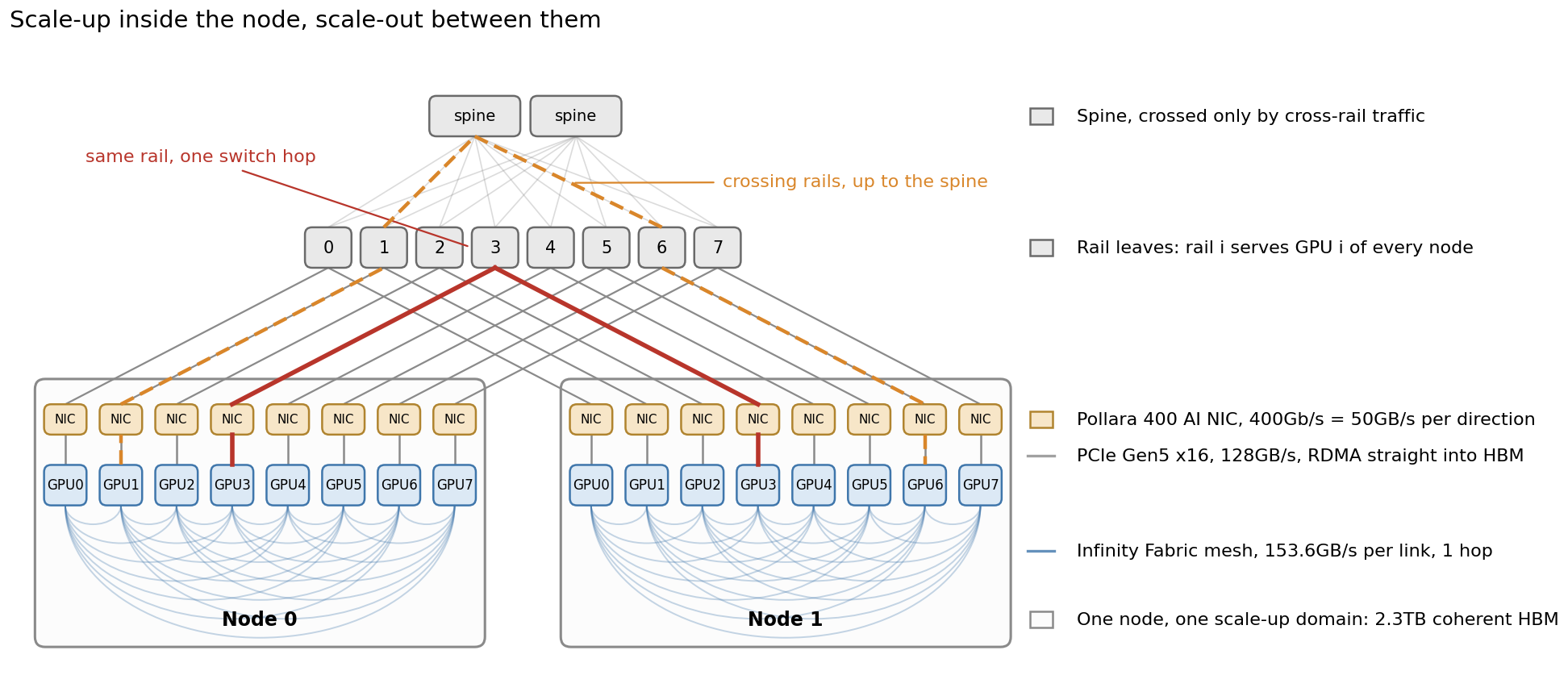
AMD’s MI3XX cluster reference design lists several NIC and switch choices. One option is a 400 Gb/s AMD Pensando Pollara 400 NIC per GPU in a RoCEv2 rail-optimized fabric. The 400 Gb/s line rate is 50 GB/s per direction before overhead:
\[\frac{400\ \mathrm{Gb/s}}{8}=50\ \mathrm{GB/s}.\]This is simply a reference design. Deployed servers may use Pollara, Broadcom, NVIDIA, or other supported RDMA adapters and they may use a fat tree, rail, or hybrid network.
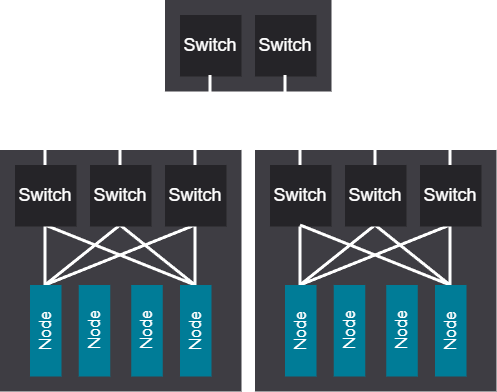
In a rail layout, GPU index $i$ on each node is paired with NIC index $i$, and equal-index NICs share a low-hop network rail. Traffic that changes rail must traverse a spine or first move over local xGMI to the correctly placed GPU. Physical mesh ordering, process ranks, and JAX mesh axes must agree before rail placement can help.
Hardware constants sheet
| Quantity | MI355X | Scope |
|---|---|---|
| Architecture target | gfx950 |
CDNA 4 |
| Form factor | OAM | UBB 2.0 platform |
| IODs | 2 | per OAM |
| XCDs | 8 | per OAM |
| Active CUs | 256 | 32 per XCD |
| SIMDs and Matrix Cores | 1,024 and 1,024 | four of each per CU |
| Wavefront width | 64 threads | wave64 |
| Maximum resident waves | 8 per SIMD | 32 per CU before resource limits |
| Peak engine clock | 2.4 GHz | ceiling, not guaranteed sustained clock |
| VGPR plus AccVGPR budget | 512 entries per lane | one shared budget per SIMD |
| LDS | 160 KiB per CU | 64 banks; 256 B/clock read peak |
| L1 vector cache | 32 KiB per CU | 128-byte lines |
| L2 | 4 MiB per XCD | 32 MiB total across eight separate slices |
| Infinity Cache | 256 MiB per OAM | shared last-level cache |
| HBM3E capacity | 288 GB per OAM | 2.304 TB across eight OAMs, not one JAX allocator |
| HBM3E bandwidth | 8 TB/s per OAM | peak theoretical |
| Dense BF16 and FP16 | 2.5166 PFLOP/s | peak theoretical |
| Dense OCP FP8 and MXFP8 | 5.0332 PFLOP/s | peak theoretical |
| Dense MXFP6 and MXFP4 | 10.0663 PFLOP/s | peak theoretical |
| BF16 machine balance | about 315 FLOP/byte | dense peak divided by HBM peak |
| Direct xGMI peers | 7 | one-hop complete graph of eight GPUs |
| xGMI per peer | 76.8 GB/s per direction | 153.6 GB/s bidirectional |
| xGMI aggregate | 537.6 GB/s per direction | all seven links active |
| PCIe | Gen 5 x16 | 64 GB/s per direction, 128 GB/s bidirectional |
| Scale-up limit | 8 GPUs | larger groups use scale-out networking |
| MI355X maximum power | 1,400 W | system cooling and power must support it |
Where these constants reappear
- Chapter 2 follows a
jax.jitcomputation from StableHLO togfx950code and identifies whether GEMMs reach MFMA library kernels. - Chapter 3 uses 288 GB, 8 TB/s, 2.5166 PFLOP/s, and directional link bandwidth to interpret XProf and ROCprofiler evidence.
- Chapter 4 compares BF16, FP16, FP8, MXFP8, MXFP6, and MXFP4 against the native matrix ceilings.
- Chapter 5 maps FSDP and expert parallelism onto the eight-GPU xGMI domain and derives their collective payloads.
- Chapter 6 measures Llama 7B rematerialization and attention routes, then follows Mixtral expert work into dense, ragged, and grouped GEMM lowerings.
References
Performance model:
- Gene M. Amdahl, “Validity of the Single Processor Approach to Achieving Large Scale Computing Capabilities” (1967). The upper bound on end-to-end speedup when only part of a workload is accelerated.
Primary hardware and architecture sources:
- AMD Instinct MI355X GPU product brief. Package, XCD and CU counts, caches, HBM, clock, precision peaks, PCIe, and xGMI.
- AMD Instinct MI355X platform brief. Eight-OAM UBB 2.0 topology and aggregate physical HBM.
- AMD CDNA 4 architecture white paper. IOD and XCD organization, execution pipelines, cache scopes, partitioning, data formats, and link derivation.
- AMD CDNA 4 ISA reference. MFMA forms, operand layouts, registers, and allocation rules.
- ROCm AMD GPU specifications.
gfx950, wave size, and per-level resource capacities. - ROCm MI350 Series architecture page. Index to the CDNA 4 ISA, white paper, and performance counters.
Primary software-facing and format sources:
- Occupancy Math on the AMD MI355X GPU. Per-SIMD register budget, per-CU LDS, wave limits, and worked occupancy arithmetic.
- FP8 GEMM Optimization on AMD CDNA 4. MFMA lane fragments, direct-to-LDS, LDS banks, and macrotile construction.
- AMD SMI GPU partitioning and ROCm workload optimization. Logical-device enumeration and MI355X SPX, DPX, QPX, CPX, and NPS pairings.
- OCP 8-bit Floating Point Specification and OCP Microscaling Formats Specification. OCP FP8 encodings, MX block size, element formats, and E8M0 scales.
- JAX explicit parallelism documentation.
jax.Arrayshardings and per-device physical storage. - ROCm GPU-enabled MPI guide. PeerDirect and GPU-aware RDMA.
- AMD Instinct MI3XX cluster reference design. Non-normative NIC, RoCEv2, tree, rail, and hybrid scale-out designs.